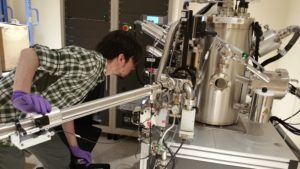
 Clemson University has installed state-of-the-art combined X-ray Photoelectron Spectroscopy (XPS) and Auger Electron Spectroscopy (AES) equipment at the multi-user Electron Microscopy Facility (EMF) in the AMRL building at Clemson University Research Park.
This capability has been highly sought by Clemson researchers working on advanced materials, bio-materials, advanced manufacturing, healthcare, digital and information technology and environmental projects. XPS and AES will directly contribute to ongoing polymer, fiber and textile research, new catalysts developments, biological implants and biomedical research, geochemical research, alternative energy technology development and all aspects of surface science-based projects at Clemson University and regional educational institutions.
Clemson faculty can schedule time for this equipment by emailing Dayton Cash at ECASH@clemson.edu. Scheduling will be accommodated on a first-come-first-serve basis. XPS/AES usage rates are posted at EMF website.
Following are some of the features of the new XPS:
- XPS Instrumentation with “scanning” monochromatic x-ray source, a motorized specimen stage, an electron energy analyzer and state-of-the-art associated electron optics.
- Small spot (<10 µm ) scanning X-ray source and imaging capabilities designed on similar approach used for electron microscopy. The instrument will be capable of producing and displaying a secondary electron (SE) image generated by the raster scanned x-ray spot. Multiple regions for further spectral analysis within the field of view will be selectable from the captured image using the instrument software, without changing the position of the specimen or translating the specimen stage.
- The instrument will be capable of <10um multi-point analysis within the FOV without moving the stage. Types of analysis include survey spectra, high-resolution spectra, and multi-point depth profiling.
- The instrument will be equipped with a 180° hemispherical electron analyzer designed for small spot sensitivity for secondary electrons, photoelectrons, and auger electrons.
- The instrument will have a charge neutralization capability that permits the analysis of electrically insulating materials. This will be based upon a dedicated adjustable low-energy electron source, which may be used in conjunction with a low-energy ion source.
- The instrument will be equipped with a computer-controlled ion gun capable of removing material from specimens by bombarding with argon (Ar) ions. This is useful during sputter depth profile experiments.
- The instrument will be equipped with a C60 cluster ion gun, adjustable up to 20 kV, aligned to sputter the specimen at the analysis point without translation of the specimen. The instrument will be capable of sputtering a mixture or alternating layers of inorganic and organic films.
- The instrument will have an electron gun controlled by the same computer and operating software to capture Auger Electron Spectra. The electron source will be capable of producing spot size <100nm for AES imaging and spectra. Switching between XPS and AES will take less than 5 seconds.
- The instrument will contain a precision five (5) axis (X, Y, Z, rotation, tilt) motorized stage. The stage will be capable of continuous motorized 360 deg. rotation during ion sputtering.
- The instrument will have a sample heating stage. The sample stage will be capable of in-situ heating and cooling from -140 C to +600 C.
- The instrument will be equipped with an automated bake out system capable of baking out the instrument. The instrument will allow the bake out time to be operator selectable, and will include automatic shutoff of the bake out system when done. The instrument will be equipped with interlocks to terminate the bake out in the event of pressure overload, ion pump failure, or excessive temperatures.
- A strong multi-year support and training from manufacturer will be in place.
For more information on this equipment and other equipment at the Electron Microscope Facility, click here.